Samsung Electronics is making every effort to expand its DRAM business to the top end for data centers. Recently, Samsung has set up an organization to boost the yield of 1b (5th generation 10-nanometer) DRAM, and plans to significantly expand production by the end of this year.
According to the industry sources, Samsung Electronics' memory division formed a separate task force(TF) last month to increase the yield of 1b DRAM.
1b DRAM refers to the 5th generation 10-nanometer DRAM with a width of 12 nanometers. Samsung started mass production of 16Gb DDR5 in May last year and succeeded in developing 32Gb DDR5 in September.
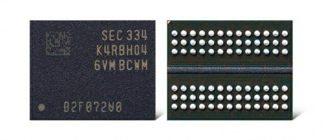
In particular, Samsung Electronics plans to introduce the 32Gb 1b DRAM as its flagship product. The DRAM is implemented in the same package size as the 16Gb product and the 128GB module can be manufactured without TSV (silicon penetration electrode) process.
In order to manufacture 128GB modules, the existing memory industry had to make a package in which two 16Gb DRAM chips are connected with TSV. If this process is omitted, manufacturing costs can be greatly reduced and power consumption can be improved by about 10%.
Samsung Electronics completed the quality test of 32Gb 1b DRAM in March and has been preparing to mass-produce it in earnest.
However, the biggest obstacle to the plan is 'yield'. Yield refers to the ratio of semiconductor good to wafer input.
It is estimated that Samsung Electronics' 1b DRAM yield has not yet reached the target yield of 80-90% of conventional DRAMs. If the yield does not reach a certain level, it is difficult for manufacturers to guarantee productivity and profitability.
In response, Samsung Electronics created a task force last month to boost yield of 1b DRAM as fast as possible. The organization is known to consist of employees in charge of all processing within its memory business unit.
At the same time, Samsung Electronics has decided to aggressively expand production of its 1B DRAM. It is understood that the company plans to expand production capacity from 40,000 per month to 70,000 in the third quarter and 100,000 in the fourth quarter, and increase it to 200,000 in the next year.
The main production bases of 1b DRAM are expected to be P2 in Pyeongtaek and 15 in Hwaseong. In particular, P2 is a 1z (3rd generation 10-nanometer DRAM) line that actively reduced production during memory recession, and the process will be actively converted.
"Samsung Electronics is making every effort to expand 1b DRAM because it can have enough production capacity compared to its competitors and does not use TSV unlike HBM (high-bandwidth memory)," an industry source said. "I understand that Jeon Young-hyun, the newly appointed DS division head, is also paying attention to improving the yield of 1b DRAM."